Journals > > Topics > Thin Films
Thin Films|545 Article(s)
Design of Self-Adaptive Thermal Control Films Based on Generative Neural Networks
Jiacheng Chen, Wei Ma, Hongyu Zhu, Yusheng Zhou, Yaohui Zhan, and Xiaofeng Li
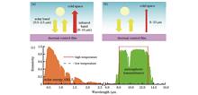
ObjectiveSelf-adaptive thermal control devices have become the research focus due to their adaptive characteristics. However, on one hand, the special spectral requirements lead to a complex and time-consuming design process, and on the other hand, the device performance needs to be optimized to meet special application scenarios. To this end, we propose a deep-generation network model to perform complex optimization tasks. Unlike traditional approaches relying on dataset updates, our model integrates a generated neural network with the transfer matrix method (TMM), which generates the expected multi-layer structure and automatically optimizes the material type and the thickness of each layer using the gradient information provided by TMM.MethodsFirstly, a neural network for global optimization is devised to intricately design the structure of photonic devices. The optimization network consists of a residual generation network and an electromagnetic solver TMM. The residual generation network obtains the refractive index and thickness of the material. The TMM solver is employed to derive the spectrum of the generated structure and compute the loss function for reverse parameter updates until the network converges. Secondly, the material categories are constrained, and the material optimization space is limited to a finite number of material properties in the specified material library. We adopt a reparameterization technique to relax the refractive index to a continuous value and restrict it to a specified position on the continuous interval with network updates. A hyperparameter is adopted to regulate the sharpness of the softmax function, thereby limiting the contribution of various materials in the material library to the specified layer. The influence of different loss functions and hyperparameters on network optimization is studied, the loss function is customized, and the best hyperparameters are selected to ensure that the network meets the requirements. Finally, a deep neural network model is utilized to optimize an adaptive thermal control device based on phase change material vanadium dioxide. The structures of 10-layer and 60-layer films are optimized, and their spectral and field distributions of the structure at high and low temperatures are studied to assess the performance.Results and DiscussionsThe proposed global optimization network model eliminates the need for a dataset and can simultaneously optimize the design of material types and thicknesses. We employ 12 materials from the material library to automatically design and optimize multi-layer film devices for adaptive thermal control on a 500 nm Ag substrate. Firstly, a 10-layer adaptive thermal control device is optimized, and the film structure is shown in Table 1. The solar absorption ratio of this device is 0.19, and the difference in high- and low-temperature emissivity is 0.79. For thin films in a high-temperature state, the electric field intensity decreases monotonically along the incident direction. Due to the top-down absorption of the thin film at this time, almost no interference between the incident and reflected waves can be observed. For thin films in a low-temperature state, the entire film system becomes semi-transparent, and strong interference between the incident and reflected waves can be observed. Increasing the number of film layers to 60 can improve device performance, which leads to a solar absorption ratio of 0.17 and 0.82 respectively (Fig. 6). When the number of membrane layers is 10, the traditional neural network's loss value continuously decreases and stops decreasing after 20 optimizations, falling into the local optimal solution and causing the gradient to disappear. Meanwhile, the global optimization network exhibits a spike in the loss value attributable to varying initial points in each optimization run, which makes the structures deviate from local optimal solutions. As the number of membrane layers increases to 60, the global optimization network yields more instances where the results diverge from local minimum values. This characteristic enables the network to effectively explore global optimal solutions and mitigates the risk of the network converging to local optimal solutions (Fig. 7).ConclusionsWe develop a global optimization network framework for designing optoelectronic devices with complex multi-layer film structures. The network solves the material classification problem by adopting probability matrices, and residual modules in the network are also leveraged to make optimization easier. As a validation and demonstration of network optimization capabilities, we adopt this method to design an adaptive thermal control device based on vanadium dioxide. This structure can automatically turn on and off radiative cooling according to environmental temperature without any additional energy input. Meanwhile, it yields excellent performance with a high-temperature solar absorption ratio below 0.2, a high-temperature emissivity greater than 0.9, and an emissivity difference greater than 0.8. Compared with traditional optimization algorithms, neural networks search for the optimal solution with high degrees of freedom and faster speed in searching for optimal solutions, underscoring the practicality of this method in complex design tasks. The results suggest the versatility of this method in designing various optoelectronic systems and highlight the potential extension of this approach to 3D photonic structures using trained neural networks, which offers possibilities for more intricate photonic device design and effective material design in diverse fields. ObjectiveSelf-adaptive thermal control devices have become the research focus due to their adaptive characteristics. However, on one hand, the special spectral requirements lead to a complex and time-consuming design process, and on the other hand, the device performance needs to be optimized to meet special application scenarios. To this end, we propose a deep-generation network model to perform complex optimization tasks. Unlike traditional approaches relying on dataset updates, our model integrates a generated neural network with the transfer matrix method (TMM), which generates the expected multi-layer structure and automatically optimizes the material type and the thickness of each layer using the gradient information provided by TMM.MethodsFirstly, a neural network for global optimization is devised to intricately design the structure of photonic devices. The optimization network consists of a residual generation network and an electromagnetic solver TMM. The residual generation network obtains the refractive index and thickness of the material. The TMM solver is employed to derive the spectrum of the generated structure and compute the loss function for reverse parameter updates until the network converges. Secondly, the material categories are constrained, and the material optimization space is limited to a finite number of material properties in the specified material library. We adopt a reparameterization technique to relax the refractive index to a continuous value and restrict it to a specified position on the continuous interval with network updates. A hyperparameter is adopted to regulate the sharpness of the softmax function, thereby limiting the contribution of various materials in the material library to the specified layer. The influence of different loss functions and hyperparameters on network optimization is studied, the loss function is customized, and the best hyperparameters are selected to ensure that the network meets the requirements. Finally, a deep neural network model is utilized to optimize an adaptive thermal control device based on phase change material vanadium dioxide. The structures of 10-layer and 60-layer films are optimized, and their spectral and field distributions of the structure at high and low temperatures are studied to assess the performance.Results and DiscussionsThe proposed global optimization network model eliminates the need for a dataset and can simultaneously optimize the design of material types and thicknesses. We employ 12 materials from the material library to automatically design and optimize multi-layer film devices for adaptive thermal control on a 500 nm Ag substrate. Firstly, a 10-layer adaptive thermal control device is optimized, and the film structure is shown in Table 1. The solar absorption ratio of this device is 0.19, and the difference in high- and low-temperature emissivity is 0.79. For thin films in a high-temperature state, the electric field intensity decreases monotonically along the incident direction. Due to the top-down absorption of the thin film at this time, almost no interference between the incident and reflected waves can be observed. For thin films in a low-temperature state, the entire film system becomes semi-transparent, and strong interference between the incident and reflected waves can be observed. Increasing the number of film layers to 60 can improve device performance, which leads to a solar absorption ratio of 0.17 and 0.82 respectively (Fig. 6). When the number of membrane layers is 10, the traditional neural network's loss value continuously decreases and stops decreasing after 20 optimizations, falling into the local optimal solution and causing the gradient to disappear. Meanwhile, the global optimization network exhibits a spike in the loss value attributable to varying initial points in each optimization run, which makes the structures deviate from local optimal solutions. As the number of membrane layers increases to 60, the global optimization network yields more instances where the results diverge from local minimum values. This characteristic enables the network to effectively explore global optimal solutions and mitigates the risk of the network converging to local optimal solutions (Fig. 7).ConclusionsWe develop a global optimization network framework for designing optoelectronic devices with complex multi-layer film structures. The network solves the material classification problem by adopting probability matrices, and residual modules in the network are also leveraged to make optimization easier. As a validation and demonstration of network optimization capabilities, we adopt this method to design an adaptive thermal control device based on vanadium dioxide. This structure can automatically turn on and off radiative cooling according to environmental temperature without any additional energy input. Meanwhile, it yields excellent performance with a high-temperature solar absorption ratio below 0.2, a high-temperature emissivity greater than 0.9, and an emissivity difference greater than 0.8. Compared with traditional optimization algorithms, neural networks search for the optimal solution with high degrees of freedom and faster speed in searching for optimal solutions, underscoring the practicality of this method in complex design tasks. The results suggest the versatility of this method in designing various optoelectronic systems and highlight the potential extension of this approach to 3D photonic structures using trained neural networks, which offers possibilities for more intricate photonic device design and effective material design in diverse fields.
Acta Optica Sinica
- Publication Date: Apr. 10, 2024
- Vol. 44, Issue 7, 0731002 (2024)

Preparation of Deep Ultraviolet High-Steepness Filter Film
Yuanhao Cai, Xiuhua Fu, Zhaowen Lin, Ben Wang, Zhuobin Huang, Yonggang Pan, Suotao Dong, and Guangyuan Fu
ObjectiveWith the rapid development of ultraviolet optics and ultraviolet technology, ultraviolet monochromator as an important tool in the development of ultraviolet technology provides strong support for related technological innovation. As an important optical component in the ultraviolet monochromator, the ultraviolet filter performance seriously affects the test accuracy of the monochromator, and its optical performance mainly includes transmittance, cut-off depth, and steepness of the transition zone, among which the influence of steepness is particularly important. In recent years, in-depth research has been carried out on the preparation of high-performance ultraviolet filter films at home and abroad, most of which focus on center transmittance, cut-off depth, and cut-off band width. Meanwhile, although the optical performance has been improved to a certain extent, in the transition zone there are still some stray rays that have not been effectively filtered out. To this end, based on the utilization requirements of the ultraviolet monochromator, a deep ultraviolet high-steepness filter film is developed to filter the interference of incoherent light and improve the measurement accuracy of the monochromator.MethodsBy analyzing material properties and studying the thin film design theory, Al2O3 and AlF3 are selected as high and low refractive index materials respectively, and a vacuum ultraviolet wide cut-off, deep ultraviolet to visible high transmission filter film is designed on the fused silica substrate by double-sided split design method. During thin film preparation, the control variable method is adopted to optimize the preparation and thin film stress analysis, and the optimal deposition process parameters are selected, which solves the problem of thin film cracking caused by excessive stress of the prepared high-steep filter film. Additionally, the monitoring error of film thickness is inverted and analyzed via repeated experiments, and the proportion coefficient of film thickness is corrected to realize the accurate monitoring of film thickness and improve the steepness of the transition zone.Results and DiscussionsDue to the large number of layers of high-steepness filter films, the accumulated stress is too large, which seriously affects the mechanical properties of the film and causes film cracking. To solve this problem, we discuss the influence of different deposition process parameters on the film quality (Table 2) and demonstrate the surface shape changes of the substrate before and after coating in Table 3. Meanwhile, the power value of the coating surface becomes larger after coating, and the residual stress of the film is expressed as tensile stress on the fused silica substrate, which is calculated by the simplified Stoney formula (Fig. 12). The process adjustment before and after increasing ion-assisted deposition energy can effectively reduce the thin film stress. Additionally, observations on the cracking degree of the film under different ion source parameters (Fig. 13) show that when the ion source power is increased to 200 V/2 A, the crack fringes of the film disappear completely, with significantly improved film properties. After the thin film deposition, the test spectral curve (Fig. 14) deviates greatly from the theoretical design spectrum. The inversion analysis reveals that this difference is mainly due to the quenching effect during the deposition of the thin film, which leads to the thin thickness of 33-54 layers, and the error inversion spectral curve is shown in Fig. 15. After repeated experiments to correct the crystallized thickness of the layer, the test spectral curve is in good agreement with the design spectral curve (Fig. 16).ConclusionsBased on the theory of thin film structure design, the reasonable selection of thin film structure parameters is realized, and the film layer thickness is appropriately adjusted and optimized, which effectively reduces film preparation difficulty. By employing the control variable method, the influence of ion-assisted deposition energy on the thin film quality is emphatically discussed. When the ion source power increases from 0 V/0 A to 200 V/2 A, the film stress decreases from 219 MPa to 178 MPa, and the problem of film cracking is effectively solved. After the thin film deposition is completed, the transmission spectrum curve is inverted and analyzed, and the proportion coefficient of the film thickness is adjusted to achieve accurate film thickness control. Finally, the deep ultraviolet high-steepness filter film has a transmittance of 3.05% at 227.7 nm, a transmittance of 89.91% at 231.3 nm, a steepness of 3.6 nm, and an average transmittance of 97.67% and 0.61% at 232-400 nm and 115-228 nm respectively, which meets the needs of the ultraviolet monochromator. ObjectiveWith the rapid development of ultraviolet optics and ultraviolet technology, ultraviolet monochromator as an important tool in the development of ultraviolet technology provides strong support for related technological innovation. As an important optical component in the ultraviolet monochromator, the ultraviolet filter performance seriously affects the test accuracy of the monochromator, and its optical performance mainly includes transmittance, cut-off depth, and steepness of the transition zone, among which the influence of steepness is particularly important. In recent years, in-depth research has been carried out on the preparation of high-performance ultraviolet filter films at home and abroad, most of which focus on center transmittance, cut-off depth, and cut-off band width. Meanwhile, although the optical performance has been improved to a certain extent, in the transition zone there are still some stray rays that have not been effectively filtered out. To this end, based on the utilization requirements of the ultraviolet monochromator, a deep ultraviolet high-steepness filter film is developed to filter the interference of incoherent light and improve the measurement accuracy of the monochromator.MethodsBy analyzing material properties and studying the thin film design theory, Al2O3 and AlF3 are selected as high and low refractive index materials respectively, and a vacuum ultraviolet wide cut-off, deep ultraviolet to visible high transmission filter film is designed on the fused silica substrate by double-sided split design method. During thin film preparation, the control variable method is adopted to optimize the preparation and thin film stress analysis, and the optimal deposition process parameters are selected, which solves the problem of thin film cracking caused by excessive stress of the prepared high-steep filter film. Additionally, the monitoring error of film thickness is inverted and analyzed via repeated experiments, and the proportion coefficient of film thickness is corrected to realize the accurate monitoring of film thickness and improve the steepness of the transition zone.Results and DiscussionsDue to the large number of layers of high-steepness filter films, the accumulated stress is too large, which seriously affects the mechanical properties of the film and causes film cracking. To solve this problem, we discuss the influence of different deposition process parameters on the film quality (Table 2) and demonstrate the surface shape changes of the substrate before and after coating in Table 3. Meanwhile, the power value of the coating surface becomes larger after coating, and the residual stress of the film is expressed as tensile stress on the fused silica substrate, which is calculated by the simplified Stoney formula (Fig. 12). The process adjustment before and after increasing ion-assisted deposition energy can effectively reduce the thin film stress. Additionally, observations on the cracking degree of the film under different ion source parameters (Fig. 13) show that when the ion source power is increased to 200 V/2 A, the crack fringes of the film disappear completely, with significantly improved film properties. After the thin film deposition, the test spectral curve (Fig. 14) deviates greatly from the theoretical design spectrum. The inversion analysis reveals that this difference is mainly due to the quenching effect during the deposition of the thin film, which leads to the thin thickness of 33-54 layers, and the error inversion spectral curve is shown in Fig. 15. After repeated experiments to correct the crystallized thickness of the layer, the test spectral curve is in good agreement with the design spectral curve (Fig. 16).ConclusionsBased on the theory of thin film structure design, the reasonable selection of thin film structure parameters is realized, and the film layer thickness is appropriately adjusted and optimized, which effectively reduces film preparation difficulty. By employing the control variable method, the influence of ion-assisted deposition energy on the thin film quality is emphatically discussed. When the ion source power increases from 0 V/0 A to 200 V/2 A, the film stress decreases from 219 MPa to 178 MPa, and the problem of film cracking is effectively solved. After the thin film deposition is completed, the transmission spectrum curve is inverted and analyzed, and the proportion coefficient of the film thickness is adjusted to achieve accurate film thickness control. Finally, the deep ultraviolet high-steepness filter film has a transmittance of 3.05% at 227.7 nm, a transmittance of 89.91% at 231.3 nm, a steepness of 3.6 nm, and an average transmittance of 97.67% and 0.61% at 232-400 nm and 115-228 nm respectively, which meets the needs of the ultraviolet monochromator.
Acta Optica Sinica
- Publication Date: Apr. 10, 2024
- Vol. 44, Issue 7, 0731001 (2024)
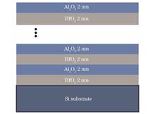
Preparation of X-Ray Multilayers Based on Atomic Layer Deposition
Lü Wensi, Hongchang Wu, Yanli Li, Xiangdong Kong, and Li Han
ObjectiveX-ray optical components are ones applied to the X-ray range and are widely employed in synchrotron radiation, free-electron lasers, high-energy astronomical observation, laboratory X-ray detection, and other scientific instruments. Among them, X-ray multilayers are important reflective optical components. Due to the short wavelength of X-rays, the multilayer period is usually in the order of a few to several tens of nanometres. In the case that the incident angle remains unchanged, the multilayer period decreases with the wavelength of X-rays. When the multilayer period is reduced to a few nanometres, the defects such as interface width and roughness will significantly reduce the X-ray reflectivity. Therefore, high-precision film preparation techniques are essential for fabricating X-ray multilayers with small periods. Several methods including ion beam sputtering, magnetron sputtering, and atomic layer deposition (ALD) have been adopted to prepare X-ray multilayers. Compared with other techniques, ALD shows advantages in achieving highly conformal films with precise control of film thicknesses on the order of angstroms. Thus, it has great potential for preparing multilayers with small periods. We study the preparation of an X-ray multilayer with small periods by the ALD method. Based on the film types that can be prepared by ALD, we calculate the X-ray (0.154 nm) reflectivity of four multilayers which consist of HfO2/Al2O3, Ir/Al2O3, Ru/Al2O3, and W/Al2O3 respectively. We also further analyze the effects of the structural parameters of multilayers on the reflectivity including periodic thickness, duty ratios, and number of periods. Based on these results, the HfO2/Al2O3 multilayer with period of 4 nm, number of periods of 60, and duty ratio of 0.5 is designed and prepared by ALD.MethodsIn the theoretical part, we adopt the Fresnel coefficient recursion method to calculate the X-ray reflectivity of multilayers with different layer materials, periodic thickness, duty ratios, and number of periods. The influence of these parameters on the X-ray reflectivity is investigated. Based on the calculated results, the HfO2/Al2O3 X-ray multilayer with periodic thickness of 4 nm, number of periods of 60, and duty ratio of 0.5 is designed. In the experimental part, ALD is applied to achieve HfO2 and Al2O3 films. For each film, in a growth cycle, two reactants are employed as precursors and they react to form films on the substrate surface in a surface self-limiting growth mode. The film thickness is controlled by the cycle numbers. As for testing methods, ThermoFisher's Scios 2 dual-beam system is adopted to obtain a cross-section sample of the multilayer that is suitable for transmission electron microscope (TEM) observation. Meanwhile, the structure of the multilayer film is observed by JEOL JEM-2100F TEM. The X-ray reflectivity of the multilayer is tested on the Beijing synchrotron radiation 1W1A line station with an X-ray wavelength of 0.154 nm. Before the test, the multilayer is placed on a horizontal stage, and the positions of the sample stage and detector are adjusted. The data of X-ray intensity at different grazing angles are acquired and fitted by IMD software. The parameters and X-ray reflectivity of the multilayer are obtained from the fitted results accordingly.Results and DiscussionsFigure 7 shows the TEM images of the cross-section of the HfO2/Al2O3 multilayer at different magnifications. The interface between HfO2 and Al2O3 is relatively sharp. However, the thickness of HfO2 is slightly larger than that of Al2O3 in one period, which indicates that a small interdiffusion exists between the layers. The results of measured and fitted X-ray reflectivity of the HfO2/Al2O3 multilayer are shown in Fig. 8. We find that two Bragg diffraction peaks appear at 1.15° and 2.23° respectively and the widths of the diffraction peaks are small, which reveals that the film deposition rate is stable and the thicknesses of each layer in the multilayer keep almost the same. By analyzing the fitted data, the X-ray reflectivity of the multilayer film is about 43%, which is a little lower than the theoretical value. The main reasons probably are the relatively large roughness of the Si substrate and the interdiffusion between the layers. For example, the roughness of the Si substrate can be transferred to the layers accumulatively, which leads to an increase in the scattering of X-rays and a decrease in the reflectivity.ConclusionsWe study the preparation of X-ray multilayers by ALD technique. X-ray (0.154 nm) reflectivity of the multilayer in ideal conditions with different layer materials and structural parameters is calculated. Additionally, we also discuss the effects of layer materials, periodic thickness, duty ratios, and number of periods on the X-ray reflectivity in detail. The calculated results show that the X-ray reflectivity of HfO2/Al2O3 multilayer with periodic thickness of 4 nm, duty ratio of 0.5, and number of periods of 60 is 53%. On this basis, the HfO2/Al2O3 multilayer film is prepared by ALD. TEM results of the multilayer show a relatively sharp interface between the layers. X-ray reflectivity results indicate that the X-ray reflectivity of the multilayer is about 43%, which shows the great potential of the ALD method for preparing X-ray multilayers with small periods. ObjectiveX-ray optical components are ones applied to the X-ray range and are widely employed in synchrotron radiation, free-electron lasers, high-energy astronomical observation, laboratory X-ray detection, and other scientific instruments. Among them, X-ray multilayers are important reflective optical components. Due to the short wavelength of X-rays, the multilayer period is usually in the order of a few to several tens of nanometres. In the case that the incident angle remains unchanged, the multilayer period decreases with the wavelength of X-rays. When the multilayer period is reduced to a few nanometres, the defects such as interface width and roughness will significantly reduce the X-ray reflectivity. Therefore, high-precision film preparation techniques are essential for fabricating X-ray multilayers with small periods. Several methods including ion beam sputtering, magnetron sputtering, and atomic layer deposition (ALD) have been adopted to prepare X-ray multilayers. Compared with other techniques, ALD shows advantages in achieving highly conformal films with precise control of film thicknesses on the order of angstroms. Thus, it has great potential for preparing multilayers with small periods. We study the preparation of an X-ray multilayer with small periods by the ALD method. Based on the film types that can be prepared by ALD, we calculate the X-ray (0.154 nm) reflectivity of four multilayers which consist of HfO2/Al2O3, Ir/Al2O3, Ru/Al2O3, and W/Al2O3 respectively. We also further analyze the effects of the structural parameters of multilayers on the reflectivity including periodic thickness, duty ratios, and number of periods. Based on these results, the HfO2/Al2O3 multilayer with period of 4 nm, number of periods of 60, and duty ratio of 0.5 is designed and prepared by ALD.MethodsIn the theoretical part, we adopt the Fresnel coefficient recursion method to calculate the X-ray reflectivity of multilayers with different layer materials, periodic thickness, duty ratios, and number of periods. The influence of these parameters on the X-ray reflectivity is investigated. Based on the calculated results, the HfO2/Al2O3 X-ray multilayer with periodic thickness of 4 nm, number of periods of 60, and duty ratio of 0.5 is designed. In the experimental part, ALD is applied to achieve HfO2 and Al2O3 films. For each film, in a growth cycle, two reactants are employed as precursors and they react to form films on the substrate surface in a surface self-limiting growth mode. The film thickness is controlled by the cycle numbers. As for testing methods, ThermoFisher's Scios 2 dual-beam system is adopted to obtain a cross-section sample of the multilayer that is suitable for transmission electron microscope (TEM) observation. Meanwhile, the structure of the multilayer film is observed by JEOL JEM-2100F TEM. The X-ray reflectivity of the multilayer is tested on the Beijing synchrotron radiation 1W1A line station with an X-ray wavelength of 0.154 nm. Before the test, the multilayer is placed on a horizontal stage, and the positions of the sample stage and detector are adjusted. The data of X-ray intensity at different grazing angles are acquired and fitted by IMD software. The parameters and X-ray reflectivity of the multilayer are obtained from the fitted results accordingly.Results and DiscussionsFigure 7 shows the TEM images of the cross-section of the HfO2/Al2O3 multilayer at different magnifications. The interface between HfO2 and Al2O3 is relatively sharp. However, the thickness of HfO2 is slightly larger than that of Al2O3 in one period, which indicates that a small interdiffusion exists between the layers. The results of measured and fitted X-ray reflectivity of the HfO2/Al2O3 multilayer are shown in Fig. 8. We find that two Bragg diffraction peaks appear at 1.15° and 2.23° respectively and the widths of the diffraction peaks are small, which reveals that the film deposition rate is stable and the thicknesses of each layer in the multilayer keep almost the same. By analyzing the fitted data, the X-ray reflectivity of the multilayer film is about 43%, which is a little lower than the theoretical value. The main reasons probably are the relatively large roughness of the Si substrate and the interdiffusion between the layers. For example, the roughness of the Si substrate can be transferred to the layers accumulatively, which leads to an increase in the scattering of X-rays and a decrease in the reflectivity.ConclusionsWe study the preparation of X-ray multilayers by ALD technique. X-ray (0.154 nm) reflectivity of the multilayer in ideal conditions with different layer materials and structural parameters is calculated. Additionally, we also discuss the effects of layer materials, periodic thickness, duty ratios, and number of periods on the X-ray reflectivity in detail. The calculated results show that the X-ray reflectivity of HfO2/Al2O3 multilayer with periodic thickness of 4 nm, duty ratio of 0.5, and number of periods of 60 is 53%. On this basis, the HfO2/Al2O3 multilayer film is prepared by ALD. TEM results of the multilayer show a relatively sharp interface between the layers. X-ray reflectivity results indicate that the X-ray reflectivity of the multilayer is about 43%, which shows the great potential of the ALD method for preparing X-ray multilayers with small periods.
Acta Optica Sinica
- Publication Date: Feb. 25, 2024
- Vol. 44, Issue 4, 0431002 (2024)
Design and Optical Characteristics of Photonic Moiré Superlattice Films
Fuyuan Zhao, and Xiaohong Sun
ObjectiveThe two-dimensional photonic Moiré superlattice (PMS) possesses some properties that conventional photonic crystals do not have, such as flat-band features and optical localization phenomena different from Anderson localization. We construct the two-dimensional photonic Moiré superlattice by multiple-beam interference and investigate its band structure and optical field properties via the finite element method. By optimizing the effects of square photonic Moiré superlattice flims (SPMSs) thickness and air-hole radius on its flat-band and localization properties, the structure of SPMSs with high localization properties is obtained. The square lattice is found to have an optical localization effect of quasi-Dirac cone different from that of the hexagonal lattice. Our study provides reference significance for the development of high-performance micro- and nanostructured devices.MethodsWe adopt MATLAB software to simulate the multiple-beam interference for preparing SPMSs, and add the threshold processing part in the algorithm to optimize the blurring phenomenon in the interferogram due to the uneven distribution of interfering light intensity. Then, square lattice photonic crystals and SPMSs with clearer structures can be obtained, and the sublattice air-hole radius r of the SPMSs can be controlled by changing the threshold value. The SPMSs model prepared uses perfectly matched layers and periodic boundary conditions. The eigenmodes and band structures are calculated using the finite element method. Comparative simulations are carried out by varying r and film thickness h to test whether these two parameters affect the local and flat band properties of SPMSs.ConclusionsOptical localization and flat-band properties exist in SPMSs as in HPMSs, while quasi-Dirac cone localization phenomena exist in SPMSs differently from HPMSs. The sublattice air-hole radius of SPMSs r and the film thickness h affect the localization and flat-band properties of SPMSs. Specifically, smaller values deform localized modes and reduce flat-band properties, and larger ones decrease the strength and flat-band properties of the localized central electric field, both of which have optimal values. Generally, SPMSs with γ of 4.98°, r of 127.5 nm, and h of 700 nm have higher-quality optical and flat-band properties. ObjectiveThe two-dimensional photonic Moiré superlattice (PMS) possesses some properties that conventional photonic crystals do not have, such as flat-band features and optical localization phenomena different from Anderson localization. We construct the two-dimensional photonic Moiré superlattice by multiple-beam interference and investigate its band structure and optical field properties via the finite element method. By optimizing the effects of square photonic Moiré superlattice flims (SPMSs) thickness and air-hole radius on its flat-band and localization properties, the structure of SPMSs with high localization properties is obtained. The square lattice is found to have an optical localization effect of quasi-Dirac cone different from that of the hexagonal lattice. Our study provides reference significance for the development of high-performance micro- and nanostructured devices.MethodsWe adopt MATLAB software to simulate the multiple-beam interference for preparing SPMSs, and add the threshold processing part in the algorithm to optimize the blurring phenomenon in the interferogram due to the uneven distribution of interfering light intensity. Then, square lattice photonic crystals and SPMSs with clearer structures can be obtained, and the sublattice air-hole radius r of the SPMSs can be controlled by changing the threshold value. The SPMSs model prepared uses perfectly matched layers and periodic boundary conditions. The eigenmodes and band structures are calculated using the finite element method. Comparative simulations are carried out by varying r and film thickness h to test whether these two parameters affect the local and flat band properties of SPMSs.ConclusionsOptical localization and flat-band properties exist in SPMSs as in HPMSs, while quasi-Dirac cone localization phenomena exist in SPMSs differently from HPMSs. The sublattice air-hole radius of SPMSs r and the film thickness h affect the localization and flat-band properties of SPMSs. Specifically, smaller values deform localized modes and reduce flat-band properties, and larger ones decrease the strength and flat-band properties of the localized central electric field, both of which have optimal values. Generally, SPMSs with γ of 4.98°, r of 127.5 nm, and h of 700 nm have higher-quality optical and flat-band properties.
Acta Optica Sinica
- Publication Date: Feb. 25, 2024
- Vol. 44, Issue 4, 0431001 (2024)
Effect of Sample Tilting Angle on the Characterization of Nanofilms by Transmission Electron Microscopy
Ge Zhang, Yun Cui, Jiaoling Zhao, Tao Wang, and Yuan'an Zhao
ObjectiveAccurate characterization of Mo/Si multilayer film thickness is important for process iteration and analysis. As one of the visualization methods, transmission electron microscopy (TEM) can characterize the thickness of nanofilm deposited on a single crystal Si wafer. It can be calibrated internally through the Si substrate lattice parameters, which is very accurate. However, if we do not pay attention to the crystal orientation of the Si substrate during TEM characterization or we use amorphous substrate materials such as fused quartz, it is difficult to ensure that the cross-section of the sample is exactly perpendicular to the electron beam. As a result, the two-dimensional projection imaging of three-dimensional samples produces artifacts, resulting in unknown measurement errors. Therefore, it is of great significance to study the influence of sample tilting angle on the TEM characterization of nanofilms.MethodsMo/Si multilayer films are deposited by pulsed direct current sputtering. Cross-section samples for TEM characterization are prepared by ion milling. TEM images and high-resolution TEM images of the multilayer films are obtained by TEM. The TEM cross-section samples are tilted in α and β directions by a double tilting holder. Combined with the profile curves of the images, we obtain the thickness of the multilayer film at different tilting angles, the roughness of the interface, and the thickness of the Mo and Si layers in a single period.Results and DiscussionsAs the Mo/Si multilayer film sample tilting in the α direction, the thickness direction of the film is always perpendicular to the electron beam direction (Z axis), so the thickness does not change. The roughness increases, because the thickness Z of the TEM sample which the electron beam passes increases as tilling in the α direction. It implies more projective superposition at the interface layer (Fig. 4). As tilting in the β direction, the sample cross-section is not perpendicular to the electron beam direction (Z axis), resulting in artifacts during projection imaging and a large deviation (Fig. 7). A formula for measuring the thickness of thin films after the sample tilting in the β direction is proposed. For thin films, the measured thickness increases with the increase of the tilting angle β. For thicker films, the measured thickness first increases and then decreases with the increase of tilting angle β. A thinner film thickness t0 causes a greater relative error of the measured film thickness after tilting in the β direction (Fig. 8).ConclusionsAs the sample tilting in the α direction, the measured thickness of the Mo and Si layers is almost unchanged while the interface roughness increases. This is because the thickness direction of the film is always perpendicular to the electron beam during rotation, and the thickness Z of the TEM sample which the electron beam through increases. The artifacts caused by the sample cross-section are not perpendicular to the electron beam during tilting, which is too severe to distinguish the Mo layer and the Si layer. The measured total thickness of the multilayer film first increases and then decreases with the increasing tilting angle. The formula for calculating the thickness of the film after the sample tilting in the β direction is presented. For thin films, the measured thickness increases with the increasing tilting angle. For thicker films, the measured thickness first increases and then decreases with the increasing tilting angle. As the film thickness t0 becomes thinner, the relative error is greater after tilting in the β direction. When the TEM sample thickness Z is 10 nm, the relative error of measuring thickness is small after tilting in the β direction. Therefore, when characterizing the structure and thickness of nanofilm by TEM, Si wafers should be cut in a specific direction [11ˉ0] from the beginning of sample preparation. Then samples should be observed from the crystal band axis [110]. Only in this way, it can ensure that the cross sections of Si wafers and films are exactly perpendicular to the electron beam. Photograph and analysis in the thin area of the TEM sample show that the result obtained by this method is more accurate. ObjectiveAccurate characterization of Mo/Si multilayer film thickness is important for process iteration and analysis. As one of the visualization methods, transmission electron microscopy (TEM) can characterize the thickness of nanofilm deposited on a single crystal Si wafer. It can be calibrated internally through the Si substrate lattice parameters, which is very accurate. However, if we do not pay attention to the crystal orientation of the Si substrate during TEM characterization or we use amorphous substrate materials such as fused quartz, it is difficult to ensure that the cross-section of the sample is exactly perpendicular to the electron beam. As a result, the two-dimensional projection imaging of three-dimensional samples produces artifacts, resulting in unknown measurement errors. Therefore, it is of great significance to study the influence of sample tilting angle on the TEM characterization of nanofilms.MethodsMo/Si multilayer films are deposited by pulsed direct current sputtering. Cross-section samples for TEM characterization are prepared by ion milling. TEM images and high-resolution TEM images of the multilayer films are obtained by TEM. The TEM cross-section samples are tilted in α and β directions by a double tilting holder. Combined with the profile curves of the images, we obtain the thickness of the multilayer film at different tilting angles, the roughness of the interface, and the thickness of the Mo and Si layers in a single period.Results and DiscussionsAs the Mo/Si multilayer film sample tilting in the α direction, the thickness direction of the film is always perpendicular to the electron beam direction (Z axis), so the thickness does not change. The roughness increases, because the thickness Z of the TEM sample which the electron beam passes increases as tilling in the α direction. It implies more projective superposition at the interface layer (Fig. 4). As tilting in the β direction, the sample cross-section is not perpendicular to the electron beam direction (Z axis), resulting in artifacts during projection imaging and a large deviation (Fig. 7). A formula for measuring the thickness of thin films after the sample tilting in the β direction is proposed. For thin films, the measured thickness increases with the increase of the tilting angle β. For thicker films, the measured thickness first increases and then decreases with the increase of tilting angle β. A thinner film thickness t0 causes a greater relative error of the measured film thickness after tilting in the β direction (Fig. 8).ConclusionsAs the sample tilting in the α direction, the measured thickness of the Mo and Si layers is almost unchanged while the interface roughness increases. This is because the thickness direction of the film is always perpendicular to the electron beam during rotation, and the thickness Z of the TEM sample which the electron beam through increases. The artifacts caused by the sample cross-section are not perpendicular to the electron beam during tilting, which is too severe to distinguish the Mo layer and the Si layer. The measured total thickness of the multilayer film first increases and then decreases with the increasing tilting angle. The formula for calculating the thickness of the film after the sample tilting in the β direction is presented. For thin films, the measured thickness increases with the increasing tilting angle. For thicker films, the measured thickness first increases and then decreases with the increasing tilting angle. As the film thickness t0 becomes thinner, the relative error is greater after tilting in the β direction. When the TEM sample thickness Z is 10 nm, the relative error of measuring thickness is small after tilting in the β direction. Therefore, when characterizing the structure and thickness of nanofilm by TEM, Si wafers should be cut in a specific direction [11ˉ0] from the beginning of sample preparation. Then samples should be observed from the crystal band axis [110]. Only in this way, it can ensure that the cross sections of Si wafers and films are exactly perpendicular to the electron beam. Photograph and analysis in the thin area of the TEM sample show that the result obtained by this method is more accurate.
Acta Optica Sinica
- Publication Date: Jan. 25, 2024
- Vol. 44, Issue 2, 0231001 (2024)

Simulation of Anti-Reflection Surfaces Constructed by Resin-Anchored SiO2 Particles
Yu Wang, Hong Lei, and Xiaohong Li
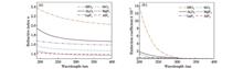
ObjectiveAnti-reflection (AR) is important in enhancing the display effect of display panels and the photovoltaic conversion efficiency of solar cells. The construction of AR structures using hollow silica (SiO2) particles (HSPs) as an effective method has been attracting related researchers. Plastic substrates, represented by polycarbonate (PC) and polymethyl methacrylate (PMMA), have broad market potential in replacing inorganic glass. However, due to the great differences between the surface properties of plastic substrates and inorganic materials, many AR coating technologies that can be easily industrialized on inorganic materials are difficult to be transferred to plastic substrates. In this context, a big challenge in constructing AR structures on plastic substrates is how to fix HSPs on organic substrates at low temperatures. Anchoring HSPs with low-temperature curable resin is a very promising strategy for industrialization with low cost and easy operation. However, the quality of AR coatings prepared by this strategy is greatly affected by the physical and chemical properties of the coating solution and the complex hydrodynamic effects during coating and drying. Many factors should be considered and optimized to obtain AR coatings with excellent performance. There are too many uncertain factors, long optimization cycle, and poor repeatability and reliability, so optimizing conditions by experimental methods willbe time-consuming and laborious. In contrast, optimizing the surface structures through simulations has incomparable advantages over traditional experimental strategies. The simulation results can point out the direction for further experimental research and accelerate experimental processes.MethodsThe effects of HSPs and HSP-solid SiO2 particle hybrid on the optical properties of as-prepared AR surfaces in the visible light range are studied by COMSOL Multiphysics. Some specific factors are examined, including the diameter of HSPs, hollowness degree, spacing between particles, resin coverage height, incidence angle, and particle arrangement pattern. A three-dimensional model is employed for simulation. The model consists of PC substrate, HSPs, resin (PMMA), and air. The minimum cell structures are studied under periodic boundary conditions. Three patterns of particle arrangements are considered (Fig. 1): square lattice arrangement, where HSPs are arranged in the X-Y plane in a square lattice; hexagonal lattice arrangement, where HSPs are arranged in the X-Y plane in a hexagonal lattice; HSP-solid SiO2 particle hybrid arrangement, where small size solid SiO2 particles are inserted into the gaps of HSP hexagonal lattice. For the square lattice arrangement, the effects of some factors on the reflectivity of the coatings are investigated, including the HSPs' size, the HSPs' hollowness degree, spacing between particles, the height of resin coverage, and incidence angle.Results and DiscussionsWhen the HSPs with a radius of 10-100 nm and hollowness of 0.7 are arranged in the form of square lattice and the resin covers half the height of the particles, coatings with low reflectance in the visible light range (380-780 nm) can be obtained (Fig. 2). The coating with the best AR effect is the one using HSPs with hollowness of 0.7. The hollowness is defined as the ratio of cavity radius to particle radius. Smaller spacing between particles facilitates lower reflectance over a broader wavelength range. When the radius of HSPs is 100 nm and the resin coverage height is 100-125 nm, the coating has the lowest reflectance in the whole visible light band (Fig. 3). The reflectance of the coatings constructed by all sizes of HSPs is lower than that of the bare PC substrate in the incidence angle range of 0°-85° (Fig. 4). For those three different patterns, the reflectance at 550 nm is 0.17% for square lattice arrangement, 0.03% for hexagonal lattice arrangement, and 0.12% for HSP-solid SiO2 particle hybrid arrangement. The average reflectance in the visible light range (380-780 nm) is 0.57% for square lattice arrangement, 0.51% for hexagonal lattice arrangement, and 0.24% for HSP-solid SiO2 particle hybrid arrangement, respectively. The changes of effective refractive indexes in the Z-direction are calculated by effective medium theory under different resin coverage heights, different degrees of hollowness of HSPs, and three particle arrangement modes. The results show that the HSP-solid SiO2 particle hybrid arrangement has one more refractive index variation gradient than the other two arrangement modes in the height of 0-40 nm (Fig. 6). However, since the effective medium theory can only qualitatively explain part of the results, the simulation via COMSOL Multiphysics is a strategy that can quickly and accurately optimize the experimental scheme of AR coatings.ConclusionsThe AR performance of coatings constructed by resin-anchored SiO2 particles is studied by COMSOL Multiphysics. The results show that the average reflectance of the coating constructed by HSPs (radius of 100 nm, hollowness degree of 0.7) arranged in a square lattice can be reduced to 0.57% in the visible light band. Compared with the bare PC substrate, the reflectance of the coating is reduced by 79.7% with the incidence angle of 0°-75°. The conditions such as hollowness degree of 0.7-0.8, resin coverage height of half the height of HSPs, and small spacing between particles are favorable to the construction of surfaces with outstanding AR performance. The hexagonal lattice arrangement of HSPs results in lower reflectivity in the 500-780 nm band, while the square lattice arrangement leads to lower reflectivity in the 380-500 nm band. When the gaps between the HSPs arranged in hexagonal lattice mode are doped with solid SiO2, the AR performance of the coating can be further improved in a broader wavelength range, and the average reflectance in the whole visible light range can be as low as 0.24%. Finally, the effective medium theory is adopted to further explore the AR mechanism of the coating. Some qualitative results are consistent with the simulation results. ObjectiveAnti-reflection (AR) is important in enhancing the display effect of display panels and the photovoltaic conversion efficiency of solar cells. The construction of AR structures using hollow silica (SiO2) particles (HSPs) as an effective method has been attracting related researchers. Plastic substrates, represented by polycarbonate (PC) and polymethyl methacrylate (PMMA), have broad market potential in replacing inorganic glass. However, due to the great differences between the surface properties of plastic substrates and inorganic materials, many AR coating technologies that can be easily industrialized on inorganic materials are difficult to be transferred to plastic substrates. In this context, a big challenge in constructing AR structures on plastic substrates is how to fix HSPs on organic substrates at low temperatures. Anchoring HSPs with low-temperature curable resin is a very promising strategy for industrialization with low cost and easy operation. However, the quality of AR coatings prepared by this strategy is greatly affected by the physical and chemical properties of the coating solution and the complex hydrodynamic effects during coating and drying. Many factors should be considered and optimized to obtain AR coatings with excellent performance. There are too many uncertain factors, long optimization cycle, and poor repeatability and reliability, so optimizing conditions by experimental methods willbe time-consuming and laborious. In contrast, optimizing the surface structures through simulations has incomparable advantages over traditional experimental strategies. The simulation results can point out the direction for further experimental research and accelerate experimental processes.MethodsThe effects of HSPs and HSP-solid SiO2 particle hybrid on the optical properties of as-prepared AR surfaces in the visible light range are studied by COMSOL Multiphysics. Some specific factors are examined, including the diameter of HSPs, hollowness degree, spacing between particles, resin coverage height, incidence angle, and particle arrangement pattern. A three-dimensional model is employed for simulation. The model consists of PC substrate, HSPs, resin (PMMA), and air. The minimum cell structures are studied under periodic boundary conditions. Three patterns of particle arrangements are considered (Fig. 1): square lattice arrangement, where HSPs are arranged in the X-Y plane in a square lattice; hexagonal lattice arrangement, where HSPs are arranged in the X-Y plane in a hexagonal lattice; HSP-solid SiO2 particle hybrid arrangement, where small size solid SiO2 particles are inserted into the gaps of HSP hexagonal lattice. For the square lattice arrangement, the effects of some factors on the reflectivity of the coatings are investigated, including the HSPs' size, the HSPs' hollowness degree, spacing between particles, the height of resin coverage, and incidence angle.Results and DiscussionsWhen the HSPs with a radius of 10-100 nm and hollowness of 0.7 are arranged in the form of square lattice and the resin covers half the height of the particles, coatings with low reflectance in the visible light range (380-780 nm) can be obtained (Fig. 2). The coating with the best AR effect is the one using HSPs with hollowness of 0.7. The hollowness is defined as the ratio of cavity radius to particle radius. Smaller spacing between particles facilitates lower reflectance over a broader wavelength range. When the radius of HSPs is 100 nm and the resin coverage height is 100-125 nm, the coating has the lowest reflectance in the whole visible light band (Fig. 3). The reflectance of the coatings constructed by all sizes of HSPs is lower than that of the bare PC substrate in the incidence angle range of 0°-85° (Fig. 4). For those three different patterns, the reflectance at 550 nm is 0.17% for square lattice arrangement, 0.03% for hexagonal lattice arrangement, and 0.12% for HSP-solid SiO2 particle hybrid arrangement. The average reflectance in the visible light range (380-780 nm) is 0.57% for square lattice arrangement, 0.51% for hexagonal lattice arrangement, and 0.24% for HSP-solid SiO2 particle hybrid arrangement, respectively. The changes of effective refractive indexes in the Z-direction are calculated by effective medium theory under different resin coverage heights, different degrees of hollowness of HSPs, and three particle arrangement modes. The results show that the HSP-solid SiO2 particle hybrid arrangement has one more refractive index variation gradient than the other two arrangement modes in the height of 0-40 nm (Fig. 6). However, since the effective medium theory can only qualitatively explain part of the results, the simulation via COMSOL Multiphysics is a strategy that can quickly and accurately optimize the experimental scheme of AR coatings.ConclusionsThe AR performance of coatings constructed by resin-anchored SiO2 particles is studied by COMSOL Multiphysics. The results show that the average reflectance of the coating constructed by HSPs (radius of 100 nm, hollowness degree of 0.7) arranged in a square lattice can be reduced to 0.57% in the visible light band. Compared with the bare PC substrate, the reflectance of the coating is reduced by 79.7% with the incidence angle of 0°-75°. The conditions such as hollowness degree of 0.7-0.8, resin coverage height of half the height of HSPs, and small spacing between particles are favorable to the construction of surfaces with outstanding AR performance. The hexagonal lattice arrangement of HSPs results in lower reflectivity in the 500-780 nm band, while the square lattice arrangement leads to lower reflectivity in the 380-500 nm band. When the gaps between the HSPs arranged in hexagonal lattice mode are doped with solid SiO2, the AR performance of the coating can be further improved in a broader wavelength range, and the average reflectance in the whole visible light range can be as low as 0.24%. Finally, the effective medium theory is adopted to further explore the AR mechanism of the coating. Some qualitative results are consistent with the simulation results.
Acta Optica Sinica
- Publication Date: May. 10, 2023
- Vol. 43, Issue 9, 0931004 (2023)
Preparation and Study of Titanium Dioxide Thin Films for Guided-Mode Resonance Filter
He Zhang, Yichen Ping, and Fei Qu
ObjectiveTitanium dioxide (TiO2) photonic crystals can be applied to prepare guided-mode resonance (GMR) filters that allow gratings to have high reflectance at resonance wavelengths. A GMR filter is a photonic crystal resonant reflector with a perfect resonant reflection of incident light with specific polarizations in arbitrarily narrow bands while allowing the light in other wavelengths to pass through. In China, few studies have been conducted on GMR filters prepared from TiO2 films. The current research on GMR filters mainly focuses on the design of GMR filters, such as sub-wavelength grating GMR filters with tunable resonance wavelengths, but their structures are more complex, which makes device fabrication difficult to be realized. In this work, a GMR filter is prepared by depositing a thin film of TiO2 on a two-dimensional patterned photonic crystal grating structure as an optical waveguide layer by atomic layer deposition (ALD). The device can produce high reflectance at the resonance wavelengths. The band of resonance wavelengths is sensitive to the refractive index of the filling material in the grating region. By controlling the refractive index of the TiO2 film, the resonance wavelength of the device can be precisely controlled, and an efficient and controllable narrow linewidth filter can be prepared.MethodsIn this present experiment, TiO2 films are deposited on a two-dimensional patterned quartz glass by the ALD technique, and then the prepared TiO2 films are annealed at different temperatures to have different refractive indices. Then we simulate the reflection spectrum of the filters by using the rigorous coupled wave algorithm (RCWA). In addition, we use a D8 X-ray diffractometer (XRD) from Bruker for the phase identification and structure analysis, a SIGMA 500 field emission scanning electron microscope (FESEM) from ZEISS for microstructure analysis, an ICON2-SYS atomic force microscope (AFM) from Bruker for surface roughness analysis, and a spectroscopic ellipsometer (SE 850 DUV) from Sentech for thickness and refractive index analysis of the thin film samples.Results and DiscussionsThe prepared TiO2 thin film samples show tetragonal anatase structure at the anneal temperatures of 200 ℃, 300 ℃, and 400 ℃, and no other characteristic peaks are found (Fig. 1). The grain sizes of the prepared TiO2 thin film samples at the anneal temperatures of 200 ℃, 300 ℃, and 400 ℃ are calculated to be 380.2 ?, 390.3 ?, and 423.6 ?, respectively, by using Scherrer's formula (Table 1). The intensity of the characteristic peaks of the TiO2 thin film samples gradually becomes higher with the increase in the annealing temperature, which indicates that the crystalline quality of the prepared samples becomes better. The FESEM and AFM photographs show that the surface of all the samples is flat and smooth, with a surface roughness of less than 0.4 nm, which indicates that the prepared thin film samples have positive denseness and flatness (Fig. 2 and Fig. 3). The thickness of the TiO2 films is 80.5 nm, 80.7 nm, and 80.8 nm after annealed at 200 ℃, 300 ℃, and 400 ℃, respectively, and the thickness of the films is independent of the annealing temperature. By changing the refractive index of the TiO2 film, the resonance wavelength of the device can be precisely controlled, and a high reflectance close to 100% at the resonance wavelength can be achieved for the application in high-efficiency narrow linewidth filters (Fig. 4). As the refractive index becomes larger, the shape of the reflection spectrum does not change, and the resonance wavelength is gradually red-shifted with resonance peaks of 946.9 nm, 959.4 nm, and 967.9 nm, respectively, and the position of the resonance peak changes within 22 nm, with full widths at half maximum of 0.74 nm, 0.77 nm, and 0.79 nm, respectively, and there is almost no change in the sideband reflectivity (Fig. 6). Therefore, by changing the refractive index of the waveguide layer TiO2 film, a narrow linewidth GMR filter can be designed for the required resonance wavelength.ConclusionsIn this paper, high-quality TiO2 films with different refractive indices are prepared on a two-dimensional patterned quartz glass by the ALD technique and annealed at different temperatures. The XRD and AFM test results show that the TiO2 films have an anatase structure, and their surface roughness is less than 0.4 nm at an annealing temperature of greater than 200 ℃. Different anneal temperatures change the refractive index of TiO2 films. The effect of the refractive index on the resonance wavelength is analyzed by the RCWA. By changing the refractive index of the TiO2 film of the optical waveguide layer, the position of the resonant peak can be effectively controlled. As a practical application example, we design a GMR filter that can control resonance wavelength in the range of 946.9-967.9 nm, and a narrow linewidth (less than 0.8 nm) is always maintained within the scope of usage. By using this method, one can achieve precise control of the resonance wavelength peak, which is beneficial to the practical application of future devices. ObjectiveTitanium dioxide (TiO2) photonic crystals can be applied to prepare guided-mode resonance (GMR) filters that allow gratings to have high reflectance at resonance wavelengths. A GMR filter is a photonic crystal resonant reflector with a perfect resonant reflection of incident light with specific polarizations in arbitrarily narrow bands while allowing the light in other wavelengths to pass through. In China, few studies have been conducted on GMR filters prepared from TiO2 films. The current research on GMR filters mainly focuses on the design of GMR filters, such as sub-wavelength grating GMR filters with tunable resonance wavelengths, but their structures are more complex, which makes device fabrication difficult to be realized. In this work, a GMR filter is prepared by depositing a thin film of TiO2 on a two-dimensional patterned photonic crystal grating structure as an optical waveguide layer by atomic layer deposition (ALD). The device can produce high reflectance at the resonance wavelengths. The band of resonance wavelengths is sensitive to the refractive index of the filling material in the grating region. By controlling the refractive index of the TiO2 film, the resonance wavelength of the device can be precisely controlled, and an efficient and controllable narrow linewidth filter can be prepared.MethodsIn this present experiment, TiO2 films are deposited on a two-dimensional patterned quartz glass by the ALD technique, and then the prepared TiO2 films are annealed at different temperatures to have different refractive indices. Then we simulate the reflection spectrum of the filters by using the rigorous coupled wave algorithm (RCWA). In addition, we use a D8 X-ray diffractometer (XRD) from Bruker for the phase identification and structure analysis, a SIGMA 500 field emission scanning electron microscope (FESEM) from ZEISS for microstructure analysis, an ICON2-SYS atomic force microscope (AFM) from Bruker for surface roughness analysis, and a spectroscopic ellipsometer (SE 850 DUV) from Sentech for thickness and refractive index analysis of the thin film samples.Results and DiscussionsThe prepared TiO2 thin film samples show tetragonal anatase structure at the anneal temperatures of 200 ℃, 300 ℃, and 400 ℃, and no other characteristic peaks are found (Fig. 1). The grain sizes of the prepared TiO2 thin film samples at the anneal temperatures of 200 ℃, 300 ℃, and 400 ℃ are calculated to be 380.2 ?, 390.3 ?, and 423.6 ?, respectively, by using Scherrer's formula (Table 1). The intensity of the characteristic peaks of the TiO2 thin film samples gradually becomes higher with the increase in the annealing temperature, which indicates that the crystalline quality of the prepared samples becomes better. The FESEM and AFM photographs show that the surface of all the samples is flat and smooth, with a surface roughness of less than 0.4 nm, which indicates that the prepared thin film samples have positive denseness and flatness (Fig. 2 and Fig. 3). The thickness of the TiO2 films is 80.5 nm, 80.7 nm, and 80.8 nm after annealed at 200 ℃, 300 ℃, and 400 ℃, respectively, and the thickness of the films is independent of the annealing temperature. By changing the refractive index of the TiO2 film, the resonance wavelength of the device can be precisely controlled, and a high reflectance close to 100% at the resonance wavelength can be achieved for the application in high-efficiency narrow linewidth filters (Fig. 4). As the refractive index becomes larger, the shape of the reflection spectrum does not change, and the resonance wavelength is gradually red-shifted with resonance peaks of 946.9 nm, 959.4 nm, and 967.9 nm, respectively, and the position of the resonance peak changes within 22 nm, with full widths at half maximum of 0.74 nm, 0.77 nm, and 0.79 nm, respectively, and there is almost no change in the sideband reflectivity (Fig. 6). Therefore, by changing the refractive index of the waveguide layer TiO2 film, a narrow linewidth GMR filter can be designed for the required resonance wavelength.ConclusionsIn this paper, high-quality TiO2 films with different refractive indices are prepared on a two-dimensional patterned quartz glass by the ALD technique and annealed at different temperatures. The XRD and AFM test results show that the TiO2 films have an anatase structure, and their surface roughness is less than 0.4 nm at an annealing temperature of greater than 200 ℃. Different anneal temperatures change the refractive index of TiO2 films. The effect of the refractive index on the resonance wavelength is analyzed by the RCWA. By changing the refractive index of the TiO2 film of the optical waveguide layer, the position of the resonant peak can be effectively controlled. As a practical application example, we design a GMR filter that can control resonance wavelength in the range of 946.9-967.9 nm, and a narrow linewidth (less than 0.8 nm) is always maintained within the scope of usage. By using this method, one can achieve precise control of the resonance wavelength peak, which is beneficial to the practical application of future devices.
Acta Optica Sinica
- Publication Date: May. 10, 2023
- Vol. 43, Issue 9, 0931003 (2023)
Design and Fabrication of Si/ZnO Multilayer Films Based on Energy Band Structure Characteristics
Jiawei Li, Xiangcheng Li, Ping′an Chen, Yingli Zhu, and Boquan Zhu
ObjectiveInfrared high reflective materials are widely employed to reduce surface emissivity. According to Kirchhoff's law, increasing the reflectivity of a material in the atmospheric window of mid- and far-infrared wavelengths can reduce the thermal radiation intensity of an object, thus decreasing the radiation difference between this object and surrounding environments. As a periodic structured functional material, photonic crystal (PC) has been extensively studied due to its extremely high infrared reflectivity and spectral compatibility. Various schemes have been designed in terms of PC film thickness and periodic structure to improve its forbidden band width and reflectance. However, there is a challenge to designing one-dimensional PCs for achieving the infrared high reflectance in 3-5 μm and 8-14 μm while minimizing the number of layers as much as possible. Therefore, this paper hopes to broaden the photonic forbidden band by constructing PC energy bands and adopting new material systems.MethodsDue to the action of the periodic potential field in semiconductor materials, electrons will form band structure and energy gaps exist between bands. However, photons in the periodic arrangement of dielectric materials will change their propagation properties and form a similar band structure. Based on Maxwell's equation, the propagation characteristics of electromagnetic waves in one-dimensional PCs are equivalent to superposition in multiple monolayer media. Since the wave vector k outside the Brillouin region is repeated, when the light wave reaches the boundary of the region, it is reflected back to the Brillouin region. After repeated reflections, a standing wave is formed, which constitutes the photonic band gap region. The upper and lower frequency regions are completely separated by the standing wave to form a photonic band gap. The light waves in the band gap cannot propagate, so the band gap in PC means high reflectance. Based on this, the transmission matrix of light waves is derived, and the PC band structure and band gap reflectance are calculated by MATLAB and CST software. According to the calculated results, the parameter is optimized and the new material system is adopted to design the one-dimensional PC model with better performance. The sample is prepared by the magnetron sputtering method for experimental verification.Results and DiscussionsFirstly, the optical properties of monolayer SiO2, ZnO, and Si films at room temperature are compared and analyzed (Fig. 3). SiO2 has a low refractive index at 3-5 μm, it is suitable as a dielectric layer in PCs. However, when the refractive index and extinction coefficient increase sharply at 8-14 μm, the PC reflectance with SiO2 as the low refractive index layer decreases greatly. The refractive index and extinction coefficient of ZnO vary less in the band of 2-14 μm, and it has a smoother reflectivity in 8-14 μm when employed as a low refractive index layer in PC (Fig. 7). In addition, the combination of one-dimensional PCs with different center wavelength structures can achieve 3-5 μm and 8-12 μm band infrared compatible high reflection. Based on this, 9-17 layers of PCs are designed and their infrared reflectances are compared (Table 1). Considering the performance of PCs and the process complexity and cost of multilayer film preparation, a 13-layer Si/ZnO one-dimensional PC is designed. The photonic band gap can be adjusted by changing the thickness of the film layer. Comparing the calculation results, it is found that the bandwidth range of each layer is optimal at one-quarter wavelength optical thickness. The structure is optimized and the final designed PC structure is shown in Fig. 7(a). The relations of the reflection spectrum with incident angle (Fig. 8) and the electric field intensity distribution of incident electromagnetic wave in PC (Fig. 9) are calculated, indicating that the structure possesses a very high infrared reflectance while being stable to the incident angle.ConclusionsIn this paper, a new one-dimensional PC for infrared high reflectance is designed based on the energy band theory. According to Maxwell's theory, the reflectances of the 3-5 μm and 8-12 μm forbidden bands of PC under the dispersion conditions are derived and calculated. A comparison of two material systems, Si/ZnO and Si/SiO2, reveals that the material with smaller dispersion can form more stable photonic forbidden bands. The selection of Si/ZnO is beneficial to achieve high infrared reflectivity in the 3-5 μm and 8-12 μm forbidden bands. Finally, a 13-layer Si/ZnO one-dimensional PC is designed and prepared. The results show that the reflectance is greater than 91.3% in the infrared bands of 3-5 μm and 8-12 μm. The experimental results are in good agreement with the simulation results, which verifies the high reliability of the model and theory. ObjectiveInfrared high reflective materials are widely employed to reduce surface emissivity. According to Kirchhoff's law, increasing the reflectivity of a material in the atmospheric window of mid- and far-infrared wavelengths can reduce the thermal radiation intensity of an object, thus decreasing the radiation difference between this object and surrounding environments. As a periodic structured functional material, photonic crystal (PC) has been extensively studied due to its extremely high infrared reflectivity and spectral compatibility. Various schemes have been designed in terms of PC film thickness and periodic structure to improve its forbidden band width and reflectance. However, there is a challenge to designing one-dimensional PCs for achieving the infrared high reflectance in 3-5 μm and 8-14 μm while minimizing the number of layers as much as possible. Therefore, this paper hopes to broaden the photonic forbidden band by constructing PC energy bands and adopting new material systems.MethodsDue to the action of the periodic potential field in semiconductor materials, electrons will form band structure and energy gaps exist between bands. However, photons in the periodic arrangement of dielectric materials will change their propagation properties and form a similar band structure. Based on Maxwell's equation, the propagation characteristics of electromagnetic waves in one-dimensional PCs are equivalent to superposition in multiple monolayer media. Since the wave vector k outside the Brillouin region is repeated, when the light wave reaches the boundary of the region, it is reflected back to the Brillouin region. After repeated reflections, a standing wave is formed, which constitutes the photonic band gap region. The upper and lower frequency regions are completely separated by the standing wave to form a photonic band gap. The light waves in the band gap cannot propagate, so the band gap in PC means high reflectance. Based on this, the transmission matrix of light waves is derived, and the PC band structure and band gap reflectance are calculated by MATLAB and CST software. According to the calculated results, the parameter is optimized and the new material system is adopted to design the one-dimensional PC model with better performance. The sample is prepared by the magnetron sputtering method for experimental verification.Results and DiscussionsFirstly, the optical properties of monolayer SiO2, ZnO, and Si films at room temperature are compared and analyzed (Fig. 3). SiO2 has a low refractive index at 3-5 μm, it is suitable as a dielectric layer in PCs. However, when the refractive index and extinction coefficient increase sharply at 8-14 μm, the PC reflectance with SiO2 as the low refractive index layer decreases greatly. The refractive index and extinction coefficient of ZnO vary less in the band of 2-14 μm, and it has a smoother reflectivity in 8-14 μm when employed as a low refractive index layer in PC (Fig. 7). In addition, the combination of one-dimensional PCs with different center wavelength structures can achieve 3-5 μm and 8-12 μm band infrared compatible high reflection. Based on this, 9-17 layers of PCs are designed and their infrared reflectances are compared (Table 1). Considering the performance of PCs and the process complexity and cost of multilayer film preparation, a 13-layer Si/ZnO one-dimensional PC is designed. The photonic band gap can be adjusted by changing the thickness of the film layer. Comparing the calculation results, it is found that the bandwidth range of each layer is optimal at one-quarter wavelength optical thickness. The structure is optimized and the final designed PC structure is shown in Fig. 7(a). The relations of the reflection spectrum with incident angle (Fig. 8) and the electric field intensity distribution of incident electromagnetic wave in PC (Fig. 9) are calculated, indicating that the structure possesses a very high infrared reflectance while being stable to the incident angle.ConclusionsIn this paper, a new one-dimensional PC for infrared high reflectance is designed based on the energy band theory. According to Maxwell's theory, the reflectances of the 3-5 μm and 8-12 μm forbidden bands of PC under the dispersion conditions are derived and calculated. A comparison of two material systems, Si/ZnO and Si/SiO2, reveals that the material with smaller dispersion can form more stable photonic forbidden bands. The selection of Si/ZnO is beneficial to achieve high infrared reflectivity in the 3-5 μm and 8-12 μm forbidden bands. Finally, a 13-layer Si/ZnO one-dimensional PC is designed and prepared. The results show that the reflectance is greater than 91.3% in the infrared bands of 3-5 μm and 8-12 μm. The experimental results are in good agreement with the simulation results, which verifies the high reliability of the model and theory.
Acta Optica Sinica
- Publication Date: May. 10, 2023
- Vol. 43, Issue 9, 0931002 (2023)
Design and Fabrication of New Curtain-Like WO3-Based Electrochromic Color-Changing Devices
Guoxin Chen, Haoyuan Chen, Zhiyong Zhang, Chenchen Zhang, Xiufeng Tang, Yunfeng Zhan, and Jianyi Luo
ObjectiveElectrochromic technology has been widely applied due to its advantages of energy conservation, environmental friendliness, intelligence, and controllability, among which the industrialization of WO3-based electrochromic devices is most mature. However, in a conventional electrochromic device consisting of upper transparent electrode ITO/counter-electrode/electrolyte/WO3/lower transparent electrode ITO, the existence of counter-electrode layers not only reduces the transmittance of the device in the bleached state but also affects its cyclic stability due to incomplete matching of the electrochemical properties between the counter-electrode layers and electrochromic layers. Though the structures of electrochromic devices have been continuously optimized, the existing counter-electrode in WO3-based electrochromic devices cannot be solved. Therefore, this paper first prepares WO3 films by magnetron sputtering and then fabricates a brand-new curtain-like electrochromic device without a counter-electrode layer based on the "current-driven model". Highly controllable color changes are achieved in the curtain-like device, and influence of the counter-electrode on device performance is eliminated because the counter-electrode is no longer required. This research can provide new pathways for structure innovation of electrochromic devices.MethodsWO3 films are fabricated by magnetron sputtering of reactive radio frequency (RF) using a W target (purity of 99.99%), an Ar flow rate of 12 sccm (1 sccm=1 m3/min), and an O2 flow rate of 4.8 sccm. The substrates are clean ITO glasses with the sheet resistance of 8 Ω/sq. The employed RF power is 80 W, and the substrate heating temperature is 200 ℃. WO3 films at different thicknesses are obtained through different sputtering durations. Meanwhile, a 1 mol/L Li ion electrolyte is prepared by dissolving LiClO4 in polycarbonate (PC) solution. Finally, the curtain-like WO3-based electrochromic devices are fabricated by sealing the ITO glass, electrolyte, and WO3 film with the UV sealant. Scanned electron microscopy images of the WO3 films are taken on a Sigma 500 instrument (Zeiss) at 10.0 kV. Phase structures of the films and ITO substrate are examined by X-ray diffraction (XRD) analysis through Cu Ka radiation (Philips X' Pert diffractometer), and X-ray photoelectron spectra (XPS) are recorded by a Thermo Fisher Scientific ESCALAB 250Xi XPS system. Finally, cyclic voltammetry (CV) tests are carried out at the voltage range of -0.8-0.8 V at a scan rate of 100 mV/s on the electrochemical workstation (CHI760E), and transmittance spectra are recorded via the UV-Vis spectrophotometer (Hitachi F-4600, Japan).Results and DiscussionsFirstly, amorphous WO3 films with the thickness of 800 nm are prepared (Fig. 1) and are preferred for ion injection and extraction. The optical modulation rate at wavelength of 550 nm is as high as 78%, and decay rate of the storage charge density is only 3.5% after 1000 CV cycles, which is far better than reported (Fig. 2). Then, curtain-like WO3-based electrochromic devices are proposed to switch between being colored and bleached without a counter-electrode under the control of a flowing current in the bottom ITO layer (Fig. 3). Bezel between the storage area and the window area of the curtain-like device is designed by introducing an artificial fissure (Fig. 4). Additionally, effect of the WO3 film thickness on the response time, recovery time and cyclic performances of the device is investigated, and the results show that the best overall performances are realized at film thickness of 800 nm (Fig. 5). The size of the storage area is also explored, and when it is similar with that of the window area, the cyclic performances could be ensured (Fig. 6). Finally, the curtain-like WO3-based electrochromic device fabricated using the above-mentioned parameters shows a higher transmittance than conventional structured ones, with excellent memory effects (Fig. 7).ConclusionsThis paper prepares high-performance WO3 films by magnetron sputtering, whose modulation rate at a wavelength of 550 nm is as high as 78%, and decay rate of the storage charge density is only 3.5% after 1000 CV cycles. Then a curtain-like electrochromic device without a counter-electrode layer is designed based on the current-driven model, where the bezel, thickness of WO3 films, and size of the ion storage area are systematically optimized. Results show that an artificially-introduced fissure in the WO3 film can simultaneously increase the response time and modulation rate of the device, and facilitates the design of the working area bezel. The overall performances of the device are best when the WO3 film is at a thickness of 800 nm. The cycling life of the device can be guaranteed when the ion storage area and the working area are similar. Finally, with the employment of optimal designing parameters, the fabricated curtain-like WO3-based electrochromic device shows excellent performances, and the transparent transmittance at a wavelength of 550 nm is 76%, which is 9 percentage points higher than that of the conventional device with an 80 nm TiO2 film as the counter-electrode. Moreover, the device also shows an excellent memory effect with the colored transmittance at 20%, only increasing by 7.5 percentage points after being placed for 10 days. These characteristics result in the great application advantages of curtain-like devices in information encryption and famous painting protection. Compared with traditional structures, the curtain-like electrochromic device features a simple structure and highly controllable color-changing patterns, which can provide guidance for the structure innovation of electrochromic devices. ObjectiveElectrochromic technology has been widely applied due to its advantages of energy conservation, environmental friendliness, intelligence, and controllability, among which the industrialization of WO3-based electrochromic devices is most mature. However, in a conventional electrochromic device consisting of upper transparent electrode ITO/counter-electrode/electrolyte/WO3/lower transparent electrode ITO, the existence of counter-electrode layers not only reduces the transmittance of the device in the bleached state but also affects its cyclic stability due to incomplete matching of the electrochemical properties between the counter-electrode layers and electrochromic layers. Though the structures of electrochromic devices have been continuously optimized, the existing counter-electrode in WO3-based electrochromic devices cannot be solved. Therefore, this paper first prepares WO3 films by magnetron sputtering and then fabricates a brand-new curtain-like electrochromic device without a counter-electrode layer based on the "current-driven model". Highly controllable color changes are achieved in the curtain-like device, and influence of the counter-electrode on device performance is eliminated because the counter-electrode is no longer required. This research can provide new pathways for structure innovation of electrochromic devices.MethodsWO3 films are fabricated by magnetron sputtering of reactive radio frequency (RF) using a W target (purity of 99.99%), an Ar flow rate of 12 sccm (1 sccm=1 m3/min), and an O2 flow rate of 4.8 sccm. The substrates are clean ITO glasses with the sheet resistance of 8 Ω/sq. The employed RF power is 80 W, and the substrate heating temperature is 200 ℃. WO3 films at different thicknesses are obtained through different sputtering durations. Meanwhile, a 1 mol/L Li ion electrolyte is prepared by dissolving LiClO4 in polycarbonate (PC) solution. Finally, the curtain-like WO3-based electrochromic devices are fabricated by sealing the ITO glass, electrolyte, and WO3 film with the UV sealant. Scanned electron microscopy images of the WO3 films are taken on a Sigma 500 instrument (Zeiss) at 10.0 kV. Phase structures of the films and ITO substrate are examined by X-ray diffraction (XRD) analysis through Cu Ka radiation (Philips X' Pert diffractometer), and X-ray photoelectron spectra (XPS) are recorded by a Thermo Fisher Scientific ESCALAB 250Xi XPS system. Finally, cyclic voltammetry (CV) tests are carried out at the voltage range of -0.8-0.8 V at a scan rate of 100 mV/s on the electrochemical workstation (CHI760E), and transmittance spectra are recorded via the UV-Vis spectrophotometer (Hitachi F-4600, Japan).Results and DiscussionsFirstly, amorphous WO3 films with the thickness of 800 nm are prepared (Fig. 1) and are preferred for ion injection and extraction. The optical modulation rate at wavelength of 550 nm is as high as 78%, and decay rate of the storage charge density is only 3.5% after 1000 CV cycles, which is far better than reported (Fig. 2). Then, curtain-like WO3-based electrochromic devices are proposed to switch between being colored and bleached without a counter-electrode under the control of a flowing current in the bottom ITO layer (Fig. 3). Bezel between the storage area and the window area of the curtain-like device is designed by introducing an artificial fissure (Fig. 4). Additionally, effect of the WO3 film thickness on the response time, recovery time and cyclic performances of the device is investigated, and the results show that the best overall performances are realized at film thickness of 800 nm (Fig. 5). The size of the storage area is also explored, and when it is similar with that of the window area, the cyclic performances could be ensured (Fig. 6). Finally, the curtain-like WO3-based electrochromic device fabricated using the above-mentioned parameters shows a higher transmittance than conventional structured ones, with excellent memory effects (Fig. 7).ConclusionsThis paper prepares high-performance WO3 films by magnetron sputtering, whose modulation rate at a wavelength of 550 nm is as high as 78%, and decay rate of the storage charge density is only 3.5% after 1000 CV cycles. Then a curtain-like electrochromic device without a counter-electrode layer is designed based on the current-driven model, where the bezel, thickness of WO3 films, and size of the ion storage area are systematically optimized. Results show that an artificially-introduced fissure in the WO3 film can simultaneously increase the response time and modulation rate of the device, and facilitates the design of the working area bezel. The overall performances of the device are best when the WO3 film is at a thickness of 800 nm. The cycling life of the device can be guaranteed when the ion storage area and the working area are similar. Finally, with the employment of optimal designing parameters, the fabricated curtain-like WO3-based electrochromic device shows excellent performances, and the transparent transmittance at a wavelength of 550 nm is 76%, which is 9 percentage points higher than that of the conventional device with an 80 nm TiO2 film as the counter-electrode. Moreover, the device also shows an excellent memory effect with the colored transmittance at 20%, only increasing by 7.5 percentage points after being placed for 10 days. These characteristics result in the great application advantages of curtain-like devices in information encryption and famous painting protection. Compared with traditional structures, the curtain-like electrochromic device features a simple structure and highly controllable color-changing patterns, which can provide guidance for the structure innovation of electrochromic devices.
Acta Optica Sinica
- Publication Date: May. 10, 2023
- Vol. 43, Issue 9, 0931001 (2023)
Organic Films with Photonic Crystals Based on Disordered Nanoparticles
Chenrui Fu, Ming Zhu, Dongxu Liu, and Da Zhao
ObjectiveThe random arrangement of dielectrics and nanostructures in disordered photonic crystals produces strong Anderson localization effect and does not require high-precision nanomaterials and structures. In the previous study, we reported photonic crystal organic films with disordered nanoparticles, which were a roll-to-roll expandable material for various applications in aerospace, automotive, construction, and apparel. However, the design parameters of disordered photonic crystals still need to be optimized. This paper aims to investigate the effect of fill factor, particle size distribution, and structural symmetry of nanoparticles on the light-insulation properties by using a finite-difference time-domain (FDTD) method. The discrete nanoparticle system of organic polymer films should be further designed by analyzing the light transport properties in the microstructure.MethodsOrganic film samples of discrete nanoparticles are prepared by using the tape casting method. The microstructure of TiO2 particles is observed by scanning electron microscopy and modeled in the FDTD. The nanostructure is simplified to a two-dimensional (2D) disordered photonic crystal in the non-polarized plane, with the particle size and the fill factor set according to experimental measurements. Electromagnetic field calculation is carried out by the FDTD method to analyze the microscopic electric field spatial distribution and macroscopic optical characteristic curves. Then the effect of different design parameters on the optical transmission characteristics is investigated. On the basis of SEM photographs, models of hierarchical size and agglomerated structures are established, and the electric field distribution of light waves in three typical structures is calculated and compared with the experimental transmittance curves. Floquet periodicity boundary conditions are set to investigate the propagation characteristics of polarized lights at different incident angles, and the wide-angle light-blocking capability is verified.Results and DiscussionsThe effects of the fill factor and particle diameter of TiO2 particles on the film spectra are investigated, and the spatial distribution of the electric field is used to describe the transmission characteristics of light waves in disordered TiO2 photonic crystals. At a fill factor of Mf=10%, the forbidden band width is wider in the range of 200-1500 nm, and the transmittance is higher. However, when Mf is larger than 45%, the forbidden band width is narrower in the wavelength range of 200-1100 nm, and the reflectance is higher at 1000 nm compared with that at a low fill factor. The results suggest that the optimal fill factor for TiO2 particles shall fall in the range of 35%-45%, so as to produce the best spectral forbidden band effect. As the nanoparticle diameter increases, the forbidden band region shifts towards the long wavelength band, and the reflection peaks become redshifted, in contrast to the blue shift observed when the fill factor increases. For a wavelength of 200 nm, the spatial electric field distribution is confined to the upper region of the array for nanoparticle diameter of 100 nm. The light of 800 nm propagates to the bottom surface of the film in the array with three particle sizes, but the phases are not synchronous. For electromagnetic waves with a length of 1600 nm, their propagation is unobstructed in the array of 100 nm, and the phase of the light reaching the bottom surface almost always reaches the wave peak, while the light reaching the bottom surface in the arrays of 200 nm and 300 nm undergoes multiple scattering and results in reduced transmittance. When the light wavelength is 3000 nm, much larger than the nanoparticle diameter, the light propagates through the film without scattering effects, the spatial distribution of the electric field is no longer influenced by the TiO2 particles, and the light transmission properties are consistent with those in a homogeneous polymer matrix. The effects of hierarchical particle size and structural aggregation on the light transmission properties are further investigated and compared with experimental results, which result in a 54% reduction in near-infrared (NIR) light transmission. Finally, the wide-angle light-blocking capability of the films is evaluated. Then the transmittance profiles and electric field spatial distribution at polarized waves are analyzed. For TE- and TM-mode polarized light, efficient band-blocking properties are achieved over a wide incidence angle range of 0°-70° for wavelengths of 200-600 nm. For a wavelength of 300 nm similar to the particle size, the light propagates only to the shallow layers of the film over a wide range of incidence angles. For a wavelength of 2000 nm, which is well beyond the particle size, TiO2 particles have difficulty in blocking light. This study provides theoretical support for the optimal design of parameters for disordered photonic crystals, especially for the preparation of organic films of TiO2 nanoparticles.ConclusionsThe preparation of disordered photonic crystal organic films is the key to achieving mass production of light-insulation materials. In this paper, hierarchically disordered photonic crystal structured organic films are designed by using thermoplastic polyurethane as the film substrate and titanium dioxide particles as the reflective barrier material filling the substrate. Simulations are carried out by using the FDTD method, and the results show that the increase in fill factor causes a blue shift in the reflection peak and spectral forbidden band, while the increase in particle diameter causes a red shift in the spectral forbidden band. Compared with arrays with a uniform distribution and a single diameter, the effects of hierarchical particle size and structural aggregation on NIR waves are analyzed. For both transverse electric and transverse magnetic waves, efficient forbidden band effects are achieved over a wide incidence angle range of 0°-70°. Such organic films containing disordered photonic crystal structures provide a reference for wide-angle light-insulation materials. ObjectiveThe random arrangement of dielectrics and nanostructures in disordered photonic crystals produces strong Anderson localization effect and does not require high-precision nanomaterials and structures. In the previous study, we reported photonic crystal organic films with disordered nanoparticles, which were a roll-to-roll expandable material for various applications in aerospace, automotive, construction, and apparel. However, the design parameters of disordered photonic crystals still need to be optimized. This paper aims to investigate the effect of fill factor, particle size distribution, and structural symmetry of nanoparticles on the light-insulation properties by using a finite-difference time-domain (FDTD) method. The discrete nanoparticle system of organic polymer films should be further designed by analyzing the light transport properties in the microstructure.MethodsOrganic film samples of discrete nanoparticles are prepared by using the tape casting method. The microstructure of TiO2 particles is observed by scanning electron microscopy and modeled in the FDTD. The nanostructure is simplified to a two-dimensional (2D) disordered photonic crystal in the non-polarized plane, with the particle size and the fill factor set according to experimental measurements. Electromagnetic field calculation is carried out by the FDTD method to analyze the microscopic electric field spatial distribution and macroscopic optical characteristic curves. Then the effect of different design parameters on the optical transmission characteristics is investigated. On the basis of SEM photographs, models of hierarchical size and agglomerated structures are established, and the electric field distribution of light waves in three typical structures is calculated and compared with the experimental transmittance curves. Floquet periodicity boundary conditions are set to investigate the propagation characteristics of polarized lights at different incident angles, and the wide-angle light-blocking capability is verified.Results and DiscussionsThe effects of the fill factor and particle diameter of TiO2 particles on the film spectra are investigated, and the spatial distribution of the electric field is used to describe the transmission characteristics of light waves in disordered TiO2 photonic crystals. At a fill factor of Mf=10%, the forbidden band width is wider in the range of 200-1500 nm, and the transmittance is higher. However, when Mf is larger than 45%, the forbidden band width is narrower in the wavelength range of 200-1100 nm, and the reflectance is higher at 1000 nm compared with that at a low fill factor. The results suggest that the optimal fill factor for TiO2 particles shall fall in the range of 35%-45%, so as to produce the best spectral forbidden band effect. As the nanoparticle diameter increases, the forbidden band region shifts towards the long wavelength band, and the reflection peaks become redshifted, in contrast to the blue shift observed when the fill factor increases. For a wavelength of 200 nm, the spatial electric field distribution is confined to the upper region of the array for nanoparticle diameter of 100 nm. The light of 800 nm propagates to the bottom surface of the film in the array with three particle sizes, but the phases are not synchronous. For electromagnetic waves with a length of 1600 nm, their propagation is unobstructed in the array of 100 nm, and the phase of the light reaching the bottom surface almost always reaches the wave peak, while the light reaching the bottom surface in the arrays of 200 nm and 300 nm undergoes multiple scattering and results in reduced transmittance. When the light wavelength is 3000 nm, much larger than the nanoparticle diameter, the light propagates through the film without scattering effects, the spatial distribution of the electric field is no longer influenced by the TiO2 particles, and the light transmission properties are consistent with those in a homogeneous polymer matrix. The effects of hierarchical particle size and structural aggregation on the light transmission properties are further investigated and compared with experimental results, which result in a 54% reduction in near-infrared (NIR) light transmission. Finally, the wide-angle light-blocking capability of the films is evaluated. Then the transmittance profiles and electric field spatial distribution at polarized waves are analyzed. For TE- and TM-mode polarized light, efficient band-blocking properties are achieved over a wide incidence angle range of 0°-70° for wavelengths of 200-600 nm. For a wavelength of 300 nm similar to the particle size, the light propagates only to the shallow layers of the film over a wide range of incidence angles. For a wavelength of 2000 nm, which is well beyond the particle size, TiO2 particles have difficulty in blocking light. This study provides theoretical support for the optimal design of parameters for disordered photonic crystals, especially for the preparation of organic films of TiO2 nanoparticles.ConclusionsThe preparation of disordered photonic crystal organic films is the key to achieving mass production of light-insulation materials. In this paper, hierarchically disordered photonic crystal structured organic films are designed by using thermoplastic polyurethane as the film substrate and titanium dioxide particles as the reflective barrier material filling the substrate. Simulations are carried out by using the FDTD method, and the results show that the increase in fill factor causes a blue shift in the reflection peak and spectral forbidden band, while the increase in particle diameter causes a red shift in the spectral forbidden band. Compared with arrays with a uniform distribution and a single diameter, the effects of hierarchical particle size and structural aggregation on NIR waves are analyzed. For both transverse electric and transverse magnetic waves, efficient forbidden band effects are achieved over a wide incidence angle range of 0°-70°. Such organic films containing disordered photonic crystal structures provide a reference for wide-angle light-insulation materials.
Acta Optica Sinica
- Publication Date: Apr. 10, 2023
- Vol. 43, Issue 7, 0731001 (2023)
Topics
© Copyright 2018-2021 | Chinese Laser Press. All Rights Reserved 沪ICP备15018463号-20